About us
FASTPCBA Co.,Ltd
-
 Building 1, Senyang Electronic Technology Park, Guangming High-tech Park, Yutang Street, Guangming District, Shenzhen City.
-
 F:86-13418481618
-
 [email protected]
 date:2019-06-28 16:16:00
Advantages and disadvantages of QFP square flat package
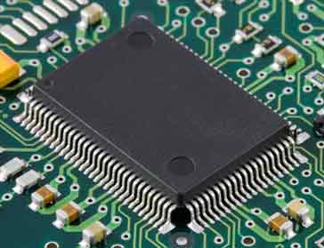
With the unprecedented improvement of large-scale integrated circuits, especially the wide application of ASICs, the pins of the chip are moving toward multi-pin and fine pitch. QFP (Quad Flat Package) is a new package developed for small-pitch surface-mount ICs. QFP is a package form that accommodates increased IC capacity and increased I/O quantity. Using a common ASIC device with a gate array.

The QFP package outline size must be an integer multiple of 5mm and 7mm, up to 40mm. The QFP pins are made of alloy. As the number of pins increases, the thickness and width of the pins become smaller. The J shape pins package is difficult. Therefore, QFP devices mostly use gull-wing pins with pin-to-center distance. 1.0mm, 0.8mm, 0.6mm, 0.5mm up to 0.3mm, etc., the number of pins is 44-160.
QFP also has a rectangular and square shape. The pin shape is gull wing, J shape and I shape. The QFP of the J-shaped pin is also called QFJ. QFP package has high soldering strength due to the large number of pins and large contact surface. However, during transportation, storage and installation, the pins are easily bent and damaged, which changes the coplanarity of the package pins, which affect coplanar soldering of component leads, so pay special attention to the usage. According to the relevant regulations, the coplanarity error of the component pins can not be greater than 0.1mm, that is, the gap difference between each pin end and the substrate is at least less than 0.1mm.
The multi-pin, fine-pitch QFP requires high precision in the SMT machine to ensure proper placement of the pads on the pins and on the board, as well as a pattern recognition system for each QFP device prior to placement. Shape identification is performed to judge the integrity and coplanarity of the component lead wires, so as to eliminate the unqualified components and ensure the solder joint quality of each pin.
Square packages are attractive to many users. The main advantage of the square package is that it enables the package to have a high density. For example, the center of the pin is 0.6 mm, larger than the square fashion and PLCC package. The number of interconnects inside the square package device is more than twice of PLCC.
Square packages also have some limitations. During transportation, operation and installation, the pins are easily damaged, and the pin coplanarity is prone to distortion, especially the pins at the corners are more susceptible to damage, and the thin body is easily broken. In shipping, each package is placed in the appropriate carrier to protect the pins, which adds significant cost.
In order to avoid these problems in square package, SMT industry has developed a special QFP device package with a gull-wing pin center-to-center spacing of 0.025 inch. The number of pins that can be accommodated is 44-244. It has a foot pad for shock absorption and is typically 3 mils longer than the pin to protect the pin from damage during handling, testing and shipping. Therefore, such packages are often referred to as "pad-like" packages.
 Building 1, Senyang Electronic Technology Park, Guangming High-tech Park, Yutang Street, Guangming District, Shenzhen City.
 F:86-13418481618
 [email protected]