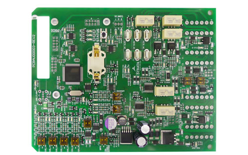
High-speed HDI board design challenges
 date:2018-11-06 18:02:00
High-speed HDI board design challenges
As information products become more and more demanding, especially the size of mobile device products is developing in the direction of continuous miniaturization. For example, the current popular Ultra Book products, even novel wearable smart devices, must use HDI high density mutual Even the technology-made carrier board further reduces the product size by the terminal design.

HDI (High Density Interconnect) is a high-density interconnect technology, which is one of the technologies used in printed circuit boards. HDI is mainly fabricated by the technique of micro-blind buried holes. The characteristic is that the distribution of electronic circuits in the printed circuit board is higher, and the density of the circuit is greatly increased, and the printed circuit board made of HDI cannot be used. Holes are formed into holes. HDI must use non-mechanical drilling processes. There are quite a few methods of non-mechanical drilling. Among them, "laser-forming holes" is the main hole-forming method for HDI high-density interconnect technology.
High-complexity integrated chips such as FPGAs and GPUs must be integrated with HDI boards because of too many pins.
When the product is extremely demanding for miniaturization, the HDI sheet can be used to compress the board area while reducing the weight.
HDI boards are designed to be more complex and require more effort to validate the design.
At present, the number of layers of HDI at a higher cost performance is mostly on the 6th floor.
At present, the number of layers of HDI at a higher cost performance is mostly on the 6th floor.
HDI printed circuit boards have a wide range of applications, such as mobile phones, ultra-thin notebook computers, tablet computers, digital cameras, automotive electronics, digital cameras, etc., have used HDI technology to reduce the motherboard design, after shrinking The benefits are quite large, not only the end product design can leave more space in the organization to the battery, or more additional functional components, the cost of the product can also be relatively reduced due to the introduction of HDI.
FASTPCBA 20 years' experience for PCB Assembly.
 Building 1, Senyang Electronic Technology Park, Guangming High-tech Park, Yutang Street, Guangming District, Shenzhen City.
 F:86-13418481618
 [email protected]
 date:2018-11-06 18:02:00

 Building 1, Senyang Electronic Technology Park, Guangming High-tech Park, Yutang Street, Guangming District, Shenzhen City.
 F:86-13418481618
 [email protected]