About us
FASTPCBA Co.,Ltd
-
 Building 1, Senyang Electronic Technology Park, Guangming High-tech Park, Yutang Street, Guangming District, Shenzhen City.
-
 F:86-13418481618
-
 [email protected]
 date:2019-06-10 10:33:00
How to solder SMT components with different solder paste heights
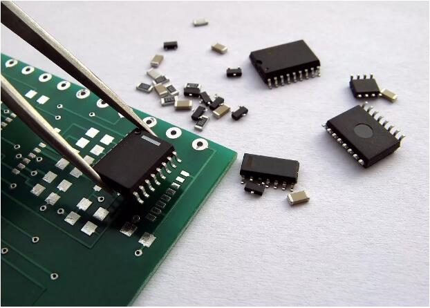
The growing demand for micro-components in SMT consumer electronics is forcing industrial electronics designers to use smaller component capsulation.

While miniaturized components offer product designers some benefits, such as energy efficiency and the ability to build more features, mixing "new and old" technologies together in the same printed circuit board PCB design can add complexity to the build stage.
This is a particular challenge for products that are “upgraded” over time, rather than considering the overall design.
Therefore, it is sometimes necessary to change the way solder paste is applied to the PCB during production. This article highlights two techniques that help overcome these potential challenges in the build process.
Why single-stage solder templates may not be suitable
In order to form a successful solder joint after reflow, it is necessary to apply solder paste at the height of the component suitable for mounting. This is controlled by the thickness of the stencil and the internal holes. For many years, templates manufacturers have had to adjust their products to reflect the growing trend of smaller, faster products. For example, we have seen eight standard thickness templates reduced to six, five, and now four.
Traditionally, applying a standard height solder paste to the entire board is sufficient to form a successful solder joint - one size (welding template) tends to fit all solder joints. However, the increasing popularity of miniaturized components used in tandem with larger components means that this solution is not always suitable. Since the solder paste height required for the same board component can now vary widely, manufacturers are increasingly finding themselves having to invest in multi-layer (or multi-height) solder paste printing techniques to avoid short circuits or open connectors risks of reflow.
At this stage, it is important to note that screen-printed solder paste is not the only option when applying solder paste to a circuit board. Solder pastes of different heights can also be dispensed at a time from the dispensing unit. However, this process is quite time consuming - for example, a medium complexity small PCB may take approximately two and a half minutes to complete compared to a screen print of about forty seconds. Therefore, electronics manufacturers must wisely consider their choices to avoid the process becoming expensive, especially if they are building large quantities of high-volume PCBA processing.
Multi-layer stage steel mesh template
Two common methods of creating multi-level templates include "stepped" and "additive" techniques. The traditional method of creating stepped templates is to start with a standard thickness - for example 5PCS - and etch away small areas to reduce the thickness of a particular component. The additive templates are generated in a similar manner - however, they start with a template of greater thickness and then etch most of the surface area to a lower thickness leaving a portion slightly above the rest. Additive templates can also be produced by laminating the various parts of the template - adding parts to make them higher - hence the name.
As with most things, there are pros and cons to using multi-level templates - no matter which way they are made. To help make decisions, you may need to consider the following factors:
1. Development time
Do you have time to test, retest and develop templates? Your first template design may not deliver solder printing perfectly. For example, if the steps produced are not large enough, the solder paste can collect in the corners of the steps as the squeegee attempts to clean the top surface of the stencil. This can be a problem in the continuous production process because you may run the risk of too much solder paste blocking the template holes, which may prevent the solder paste from flowing smoothly through the opening and reducing the level of transfer on the PCB. Therefore, you may need to redesign and retest the template until the correct size is reached, which makes the template design process costly and time consuming.
2. The proximity degree of hybrid technology
As already discussed, the multilayer portion needs to be large enough to enable the squeegee to adequately clean the top surface of the stencil. This may mean that you have to find holes in other parts of the etched part. However, this may also mean that these additional components will achieve a lower height solder paste consistent with the miniaturized components, which may not be sufficient.
3. Cost
Given the time, labor, and template design process, creating a perfect multi-layer template can be an expensive job. If you plan to produce medium to large quantities of PCBs on a regular basis, you may find that upfront costs can quickly recover costs. However, if you decide to use another method (such as manual placement), you need to consider the extra time and costs associated with this method.
Direct flux application
Direct flux applications as soldering technology can only be used for ball grid array (BGA) components - regardless of size. Applying the correct level of flux to the BGA presents a similar challenge for applying the correct level of solder paste to the PCB. Too much, the gap between the joints can fill the reflowed flux residue, limiting the ability to fill the assembly. Also, not enough flux and solder will not flow to the optimum state, and you may leave a dry or open joint. Based on experience, we recommend covering 50-75% of the solder ball height in the flux.
 Building 1, Senyang Electronic Technology Park, Guangming High-tech Park, Yutang Street, Guangming District, Shenzhen City.
 F:86-13418481618
 [email protected]