About us
FASTPCBA Co.,Ltd
-
 Building 1, Senyang Electronic Technology Park, Guangming High-tech Park, Yutang Street, Guangming District, Shenzhen City.
-
 F:86-13418481618
-
 [email protected]
 date:2019-12-03 15:38:02
In PCB manufacturing,component layout direction of wave soldering process
(1) In order to make both ends of the PCB manufacturing components contact the solder wave at the same time, the long axis of the chip component should be perpendicular to the direction of the wave soldering machine.

(2) The long axis of the SMD device should be parallel to the conveyor belt direction of the wave soldering machine.
(3) In order to avoid shadow effects, the ends of components of the same size are arranged in a line parallel to the wave soldering transmission direction; components of different sizes should be staggered and should not be lined up. Small-sized components should be arranged In front of the large component, prevent the component body from blocking the soldering terminal and the soldering pin. When it is not possible to arrange according to the above requirements, a space of 3 ~ 5mm should be left between the components.
(4) The characteristic directions of components should be consistent.
(5) When using PCB manufacturing wave soldering process, several points of PCB design are as follows
① Elliptical pad patterns should be used for high-density wiring to reduce solder bridge.
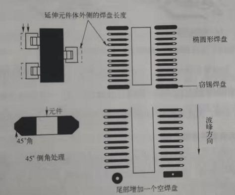
② In order to reduce the shadow effect and improve the welding quality, when designing the land pattern of wave soldering, the pad length of rectangular components SOT and SOP components should be processed as follows

Extend the pads outside the component for extension treatment;
Widen the two pairs of pads on the outermost side of the SOP to attract excess solder (commonly known as theft pads);
Rectangular components smaller than 3.2mmx 1.6mm can be chamfered at 45 ° on both sides of the pad.
③ In wave soldering, the via should be set at the tail of the pad or close to the pad. The position of the via hole should not be covered by the component to facilitate gas discharge. When the via is set on the pad, the general hole is 0.254mm away from the component tip.
The arrangement direction and order of components follow the following principles. The component layout and arrangement direction should follow the principle of smaller components in front and try to avoid blocking each other. The large and small components on the wave soldering surface should be staggered and not lined up. Do not place QFP, PLCC and other devices with pins on four sides. In special cases such as single panel, QFP must be placed on the wave side.
Because the chip components have been mounted on the PCB before wave soldering, the position will not be moved during wave soldering, so the shape, size, symmetry requirements of the PCB manufacturing pads, and the connection between the pads and the wires can be more flexible.
 Building 1, Senyang Electronic Technology Park, Guangming High-tech Park, Yutang Street, Guangming District, Shenzhen City.
 F:86-13418481618
 [email protected]