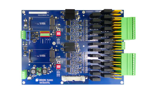
Key components with high pin counts require HDI for product design
 date:2018-11-06 18:05:00
Key components with high pin counts require HDI for product design
In particular, FPGA components with a large number of pins are extremely troublesome for PCB layout. For example, the most common GPU components at present, the number of pins is also increasing, and most of them have been changed to HDI printed circuit boards. For product design, HDI is especially suitable for designs that require highly complex connections.
Especially for a new generation of SoCs or integrated chips, the highly integrated function leads to more and more IC pins, which makes the PCB design connection line more difficult, and the HDI high-density circuit board design can utilize multiple layers inside the board. The advantages of interconnection and integration are to connect the complicated wafer pins one by one, and the laser blind hole fabrication can make micro blind holes in the plate, which can be perforated, misplaced, stacked, or in any layer. For interconnects, the layout flexibility of the lines is much higher than that of conventional PCBs, and it provides an easier sheet design for integrated chip applications with high pin counts.

The HDI board design is more complicated than the previous PCB, not only the line becomes more compact, but also the design complexity of using different layers of circuit interconnection is greatly improved, and the line becomes finer and tighter, which also represents The change in the conductor cross-sectional area of the line is small, which will lead to a more prominent problem of transmitting signal integrity. It is necessary for the PCB design engineer to pay more attention to the verification and troubleshooting of the board function.
Especially in the case of highly complex design cases, such as the possibility of design changes in the electronic circuit of the board during the development process, if the core components of the motherboard have FPGA or other components with a large number of pins, a little design change It will cause the design to improve the time delay, and how to minimize the line deployment error during the frequent design change process, must be matched with the design aids that can support the HDI high complexity circuit design, especially the logic that can be matched in the FPGA. Design, hardware design, PCB logic and related design data can communicate with each other. The design specifications of any project can be instantly reflected in the development system to avoid design problems that cannot be matched between the design board and the target wafer.
FASTPCBA 20 years' experience for PCB Assembly.
 Building 1, Senyang Electronic Technology Park, Guangming High-tech Park, Yutang Street, Guangming District, Shenzhen City.
 F:86-13418481618
 [email protected]
 date:2018-11-06 18:05:00

 Building 1, Senyang Electronic Technology Park, Guangming High-tech Park, Yutang Street, Guangming District, Shenzhen City.
 F:86-13418481618
 [email protected]