About us
FASTPCBA Co.,Ltd
-
 Building 1, Senyang Electronic Technology Park, Guangming High-tech Park, Yutang Street, Guangming District, Shenzhen City.
-
 F:86-13418481618
-
 [email protected]
 date:2020-11-24 09:46:02
The film bottom plate is the leading process of PCB production. In the production of a certain kind of PCB, at least one film backplane should be provided for each electrical pattern (signal layer circuit pattern and ground, power layer pattern) and non-conductive pattern (solder resistance pattern and characters) of the PCB. The use of film substrate in PCB production is the photosensitive mask pattern in pattern transfer, including circuit pattern and photoresist pattern; the production of screen film in screen printing process, including solder mask pattern and characters; machining (drilling and Shape milling) CNC machine tool programming basis and drilling reference.
Substrate material Copper Clad Laminaters, CLL, referred to as copper clad layer or copper clad laminate, is the substrate material for manufacturing PCB. At present, the most widely used PCB made by etching method is to selectively etch on the copper clad board to obtain the required circuits and patterns.
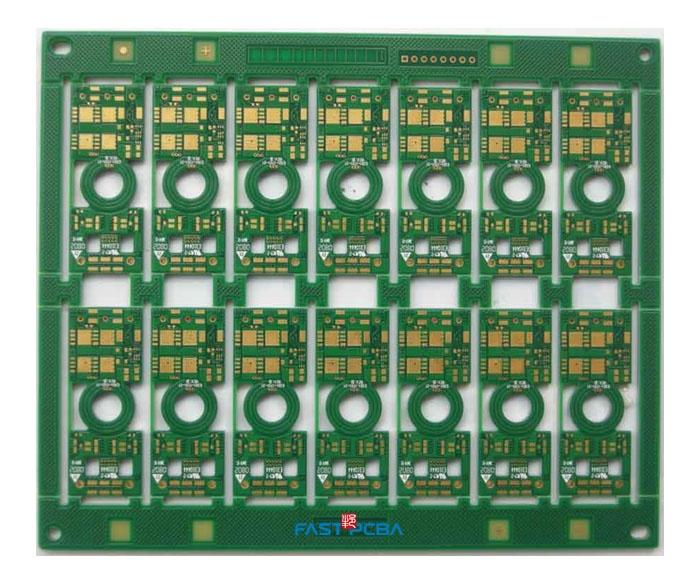
After the PCB design of imposition and light drawing data generation is completed, because the PCB board is too small to meet the production process requirements, or a product is composed of several PCBs, it is necessary to combine several small boards into a large board with an area that meets the production requirements. You need to make a film base map first, and then use the base map to take pictures or reprint. With the development of computer technology, printed board CAD technology has made great progress, and the level of PCB production technology has continued to increase rapidly in the direction of multi-layers, thin wires, small holes, and high density. The original film manufacturing process can no longer meet the requirements of PCB. The design is needed, so the light drawing technology appeared. Using the light drawing machine, the PCB graphic data file designed by CAD can be directly sent to the computer system of the light drawing machine. The light drawing machine uses the light to directly draw the graphics on the negative film, and then develop it. Fix to get the film master.

The generation of gerber data is to convert the design data generated by CAD software into gerber data (mostly Gerber data), which is modified and edited by the CAM system to complete the gerber pre-processing (imposition, mirroring, etc.) to achieve According to the requirements of the PCB production process, the processed data is then sent to the light plotter, which is converted into raster data by the light image data processor of the light plotter, and this raster data is sent to the laser light plotter through a high-speed compression reduction algorithm. Finish light painting.
For 20 years, FASTPCBA has focused on PCB manufacturing and SMT assembly.
Offering:
1) PCB Assembly
2) Rigid PCB (1~48Layer)
3) Flexible PCB
4) Rigid-flex PCB
5) HDI PCB
6) Gold-Plated PCB
7) High Frequency PCBs
...
 Building 1, Senyang Electronic Technology Park, Guangming High-tech Park, Yutang Street, Guangming District, Shenzhen City.
 F:86-13418481618
 [email protected]