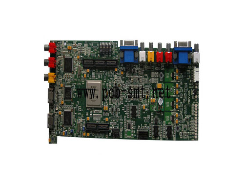
PCB Layout design flow
 date:2018-11-05 15:50:00
PCB Layout design flow
There are some basic PCB concepts before you start teaching software. First of all, there must be an idea. The PCB talks about the manufacturing process, not the circuit design. So even if you don't know much about circuit design, you can basically make a PCB board as long as you have a working circuit diagram. You can also make your own PCB board as long as you have mastered some of the Design Rules.

As for how to determine that this is a circuit diagram that can be "worked"? You can first verify the circuit with a hole plate or use a breadboard to insert a plug, first make sure that this is working... Layout PCB, IC parts Then choose the version of SMD)
To complete a PCB board, it can be basically divided into three main stages, the first stage circuit diagram drawing, the second stage circuit layout, and the third stage is to build a BOM table, and then prepare materials for hand and hand soldering.
If your PCB needs to be laid out above 4 layers or high speed, RF, antenna such as high frequency, this is already pro professional level, it is not easy without expert guidance, plus you don't have too many measuring instruments. Some are also unlikely to do it themselves. This is another level. It is recommended to find a Layout House OEM with relevant design expertise, because there may be EMI, FCC, CE, and NCC specifications.
FASTPCBA 20 years' experience for PCB Assembly.
 Building 1, Senyang Electronic Technology Park, Guangming High-tech Park, Yutang Street, Guangming District, Shenzhen City.
 F:86-13418481618
 pcba13@fastpcba.cn
 date:2018-11-05 15:50:00

 Building 1, Senyang Electronic Technology Park, Guangming High-tech Park, Yutang Street, Guangming District, Shenzhen City.
 F:86-13418481618
 pcba13@fastpcba.cn