About us
FASTPCBA Co.,Ltd
-
 Building 1, Senyang Electronic Technology Park, Guangming High-tech Park, Yutang Street, Guangming District, Shenzhen City.
-
 F:86-13418481618
-
 [email protected]
 date:2019-11-08 11:35:09
The factors that pcb manufacturing affects solder paste printing include three aspects, namely solder paste performance, stencil and printing process.

Solder paste properties include:
1.Viscosity
2.Thixotropic index
3. Alloy powder weight percentage
4. Alloy powder particle size
5. The shape of the alloy powder
Templates include:
1. Selection of template thickness
2. Template material selection
3. Opening size, hole wall roughness
The printing process includes:
1.Scraper speed
2. Scraper shape and material
3. Scraper pressure
4. Separation speed
5. Separation distance
6. Printing support
7. Wipe the network settings
Solder paste performance
1, Viscosity
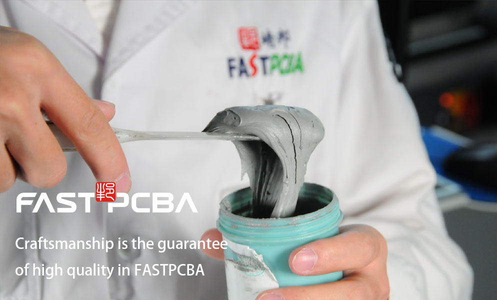
The rheological properties of pcb manufacturing solder paste are the main factors affecting solder paste filling and transfer, while the main parameters characterizing the rheological properties of solder paste are viscosity and thixotropy. Solder paste viscosity is the main rheological property of solder paste, which not only affects the filling of solder paste, but also affects the transfer of solder paste.
2. Thixotropy
Thixotropy refers to the performance of fluid shear stress decreasing with time under a certain shear rate, and is generally characterized by a thixotropic index.
The excellent solder paste has a high thixotropic index, that is, the solder paste has a low viscosity at a high shear rate and a high viscosity at a low shear rate. The high thixotropic index solder paste has excellent printability, and the printed pattern has high resolution, and the solder paste pattern collapses small to better maintain the shape of the pattern.
3. Alloy content
The effect of alloy content on solder paste is still essentially the effect on viscosity.
4.Solder powder particle size
The particle size of the solder alloy powder has a great influence on the transfer rate of the solder paste and the regularity (or resolution) of the solder. According to experience, the particle size of the solder powder should match the opening size and thickness of the template. Solder paste is selected based on the number of solder balls accommodated in the width and height dimensions of the stencil opening.
Here, a concept is proposed, which is called the hole wall effect at present. The influence of the hole wall on the pattern transfer must be related to the size of the template thickness solder alloy particles. For example, the hole wall only affects the distance of one solder ball. Obviously, the larger the opening size or the smaller the solder particle size of pcb manufacturing, the smaller the effect of the hole wall on the solder paste pattern, which should be the reason why the opening size should match the solder particles. The reason why 0.4mm BGA (CSP) is easy to appear is that it is related to the distance and length of the hole wall solder paste pattern. The opening size is small and the circumference has a hole wall, which is obviously not conducive to the transfer of solder paste, and the resistance is relatively large. The 0.4mm QFP solder paste pattern is prone to projection at both ends, which is also the reason for the large hole wall effect.
Therefore, for the assembly of fine pitch components, the template should be thin and not thick, and the size of the solder powder should be small and not large. The smaller the solder paste particle size, the better the printing effect and the smaller the effect of the hole wall effect.
Template factor
The area ratio of the template, the roughness of the template hole wall and the hole shape mainly affect the transfer rate of the solder paste.
The so-called area ratio refers to the ratio of the open area of the template to the area of the open hole wall. The area ratio is an important factor affecting the transfer rate of pcb manufacturing solder paste. Generally, the area ratio is greater than 0.66, and more than 70% transfer rate can be obtained under this condition.
The area ratio essentially reflects the effect of the amount of tin on the sidewall when the template is demolded. When the solder paste is demolded, whether the solder paste filled into the template opening can be completely transferred to the PCB pad depends on the roughness of the sidewall and the viscosity of the solder paste. Obviously, the larger the area ratio, the smaller the ratio of the template to the transfer rate of the solder paste, that is, the smaller the wall effect phenomenon described above, the smoother the opening sidewall and the easier the transfer.
Printing parameters
Solder paste printing parameters mainly refer to the setting parameters of the blade speed, blade angle, separation speed, separation distance and so on. The blade speed, the blade angle and the secondary knife pressure mainly affect the filling of the solder paste. The separation speed and the separation distance mainly affect the transfer of the solder paste.
 Building 1, Senyang Electronic Technology Park, Guangming High-tech Park, Yutang Street, Guangming District, Shenzhen City.
 F:86-13418481618
 [email protected]