About us
FASTPCBA Co.,Ltd
-
 Building 1, Senyang Electronic Technology Park, Guangming High-tech Park, Yutang Street, Guangming District, Shenzhen City.
-
 F:86-13418481618
-
 [email protected]
 date:2020-09-10 16:55:34
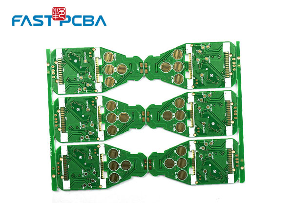
pcb puzzle is only for the convenience of production. For board manufacturers, their base materials are generally relatively large. They make many boards at a time, and then cut them one by one. If the jigsaw is mainly used for welding production, Imagine a board with a large fingernail is welded one by one on an SMT machine the size of a car.

There are several definitions of pcb puzzle.
1. Convenient for customer plug-ins;
Convenience plug-in is what the customer requires, and you must do it as required.
2. Convenient for manufacturers to produce by themselves;
The convenience of the manufacturer is to facilitate V-cutting and so on.
3. Save materials;
Saving materials is for more perfect use of materials without wasting or leaving too much side material! For example, with a material of 1.2m*1m, you will be perfect when you open a 34*41CM puzzle.
pcb puzzle method
PCB splicing methods, including the use of Excel programs stored in well-known computers to create finished board splicing worksheets and blank splicing worksheets, and the use of the above worksheets; finished board splicing worksheets are used to complete the finished product The process of slabs in the same phase and different phases of the slabs. Each column of the finished slab paneling worksheet is used to place the data of the same category of different slab paneling schemes or the Excel internal function calculation formula of the data, each row Cells are used to place different types of data of the same puzzle plan or Excel internal function calculation formulas for the data. The specific method to create a finished board puzzle worksheet is:
(1) Start the Excel program stored in a known computer, create a new workbook, and select a worksheet;
(2) Use a cell in the table to enter the name of the worksheet:
(3) Use a row of cells in the table as the header of the worksheet, and enter the category name of the data in the column in each cell;
(4) Create a data input area:
(5) Create data operation area
(6) Create data output area
(7) Create a puzzle operation area
(8) Create an indirect output area. Use Excel's internal search and reference functions to reference all data in the worksheet of the puzzle operation area and place it in the indirect output area.
PCB puzzle skills
PCB splicing is something that PCB manufacturers often do. What matters should be paid attention to when making splicing? What are the key rules for PCB puzzle? To summarize for you as follows:
The first is the problem of puzzle. We know that the main problem of puzzle is to save production costs. For PCB panel width ≤260mm-300mm, it varies according to different production lines. Because we may have a lot of materials, one material gun corresponds to one module in our processing equipment, so if the puzzle exceeds the range of the module, the processing speed will become very slow.
The outer frame (clamping side) of the PCB panel should be carefully considered to ensure that the PCB panel will not be deformed after being fixed to the fixture (generally, it is not allowed to open V grooves on this side). The orientation should be consistent, and there can be no mirror image, which will cause the coordinate positioning problem of processing.
Second, at the edge (between the outer frame of the jigsaw panel and the inner small board, and between the small board and the small board), there should be no connector extension. If this situation exists, it will prevent the tool from separating after the welding is completed.
In order to ensure the position and level of the detection board, we need to set more than three positioning points on the edge of the board. By optically detecting these three points, the reference coordinates of the entire processing and the level of the board can be obtained.
The correct approach is to set the distance 5mm from the edge and the direction of travel is inconsistent (to distinguish the direction of entry): When setting the reference positioning point, usually leave a non-resistance area 1.5 mm larger than it around the positioning point, which cannot be similar Pads or other similar
There must be at least three positioning holes in each small board, 3≤aperture≤6 mm, and no wiring or patching is allowed within 1mm of the edge positioning hole (to prevent misjudgment). PCB boarding is mainly to save production and processing costs (making the machine processing speed several times faster). Unreasonable design will make the later stage full of problems. You can take a closer look to prevent problems.
The first is the problem of puzzle. We know that the main problem of puzzle is to save production costs. For PCB panel width ≤260mm-300mm, it varies according to different production lines. Because we may have a lot of materials, one material gun corresponds to one module in our processing equipment, so if the puzzle exceeds the range of the module, the processing speed will become very slow.
 Building 1, Senyang Electronic Technology Park, Guangming High-tech Park, Yutang Street, Guangming District, Shenzhen City.
 F:86-13418481618
 [email protected]