About us
FASTPCBA Co.,Ltd
-
 Building 1, Senyang Electronic Technology Park, Guangming High-tech Park, Yutang Street, Guangming District, Shenzhen City.
-
 F:86-13418481618
-
 [email protected]
 date:2019-07-05 18:10:00
What materials are mainly assembled from PCB boards?
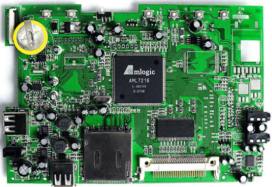
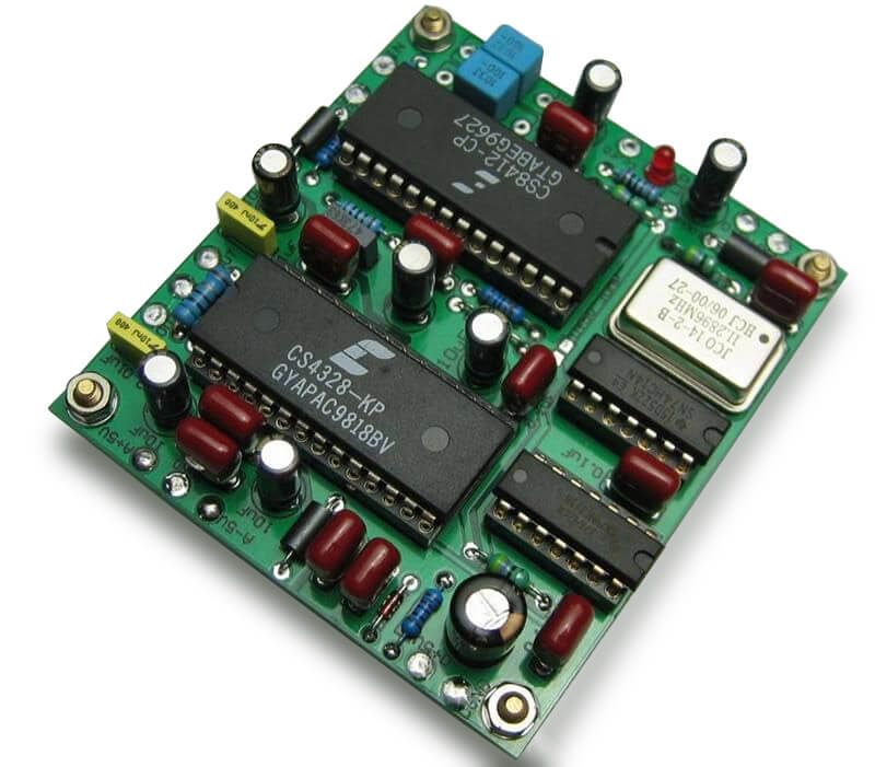
PCB boards are a bit like layer cakes or lasagna, with alternating layers of different materials that are laminated together with heat and adhesive so that the result is a single object.

FR4 substrate
The substrate is typically a glass fiber. Historically, the most common sign of this fiberglass is "FR4." This rugged core gives the PCB board rigidity and thickness. There is also a flexible PCB board built on flexible high temperature plastic.
Cheaper PCB boards and perforated sheets will be made from other materials, such as epoxy or phenolic resins, which lack the durability of FR4 but are much less expensive. When you solder it, you will know that you are using this type of PCB - they have a very unpleasant smell. These types of substrates are also commonly found in low-end consumer electronics. Phenolic resins have a lower thermal decomposition temperature which causes delamination, smoke and charring when the soldering iron remains too long on the board.
Copper
The next layer is a thin copper foil laminated to the board with heat and adhesive. On a conventional double-sided PCB board, copper is applied to both sides of the substrate. In lower cost electronic devices, the PCB board may have copper on only one side. When we refer to double-sided or double-layer boards, we refer to the number of copper layers in the lasagna. This can be 1 or up to 16 or more layers.
Copper thickness can vary and is expressed in ounces per square foot by weight. Most PCBs have 1 ounce of copper per square foot, but some PCBs that handle very high power may use 2 or 3 ounces of copper. Converted to about 35 microns or 1.4 thousandths of an inch thick copper per square ounce.
Solder mask
The layer on top of the copper foil is called a solder mask. This layer makes the PCB board green (or, in SparkFun, red). It covers the copper layer and insulates the copper trace from accidental contact with other metals, solder or conductive sites. This layer helps the user solder to the correct location and prevent solder jumpers.
Silk screen
A white screen layer is applied on top of the solder mask layer. Screen printing adds letters, numbers and symbols to the PCB board to facilitate assembly and to give people a better understanding of the board. We often use screen labels to indicate the function of each pin or LED.
Screen printing is most commonly white, but any ink color can be used. Black, gray, red, and even yellow screen printing colors are widely available; however, it is not uncommon to see multiple colors on a single board.

The approximate composition of the above PCB boards, many of the circuit boards are expensive in the process, and there is material selection.
 Building 1, Senyang Electronic Technology Park, Guangming High-tech Park, Yutang Street, Guangming District, Shenzhen City.
 F:86-13418481618
 [email protected]